Acroview technology
800V HVDC and the Power Scaling Limits of AI Infrastructure
Executive Summary
AI model scaling is shifting the primary constraint in data center design from compute density to power delivery.
Rack power consumption is increasing at a rate that exceeds the limits of conventional 54 V DC distribution architectures.
The industry, including NVIDIA and OCP ecosystem partners such as Infineon, Schneider Electric, and Vertiv, is moving toward 800 V HVDC deployment, targeting production-scale adoption around 2027.
This transition represents a change in power architecture domains, not an incremental optimization.
1. 54 V architecture limits at system scale
AI workloads are driving a step change in rack-level power density:
- Hopper (H100/H200): ~40 kW per rack
- Blackwell (GB200 NVL72): 120–130 kW per rack
- Next-generation Rubin-class systems: >200 kW per rack, extending toward 1 MW-class racks
At 1 MW rack power, 54 V distribution requires current levels approaching 18,500 A.
At this operating point, three constraints dominate system design.
3. Power conversion hierarchy
AI accelerators require sub-1 V core supply voltage, requiring a multi-stage conversion chain.
3.1 10 kV AC → 800 V DC (facility level)
Solid-state transformers (SST) or medium-voltage rectification systems replace traditional transformer-based architectures.
Silicon carbide (SiC) devices enable direct conversion from medium-voltage AC to 800 V DC with efficiency above 98%.
3.2 800 V DC → 48 V / 54 V DC (rack level)
Rack-level power is implemented through sidecar architectures, separating power conversion from compute infrastructure.
High-ratio LLC resonant converters operate under ZVS/ZCS conditions to reduce switching losses.
3.3 48 V DC → 12 V DC (board level)
Gallium nitride (GaN) devices operating in the MHz switching range enable high-density conversion.
Higher switching frequency reduces passive component size and increases power density.
3.4 12 V DC → sub-1 V GPU rail (point-of-load)
GPU power delivery requirements reach multi-kiloampere current levels at sub-1 V voltage.
Lateral power delivery (LPD) is replaced by vertical power delivery (VPD).
VRM modules are placed directly beneath the GPU package.
Electrical path length is reduced to millimeter scale.
Power delivery efficiency improves by ~5%.
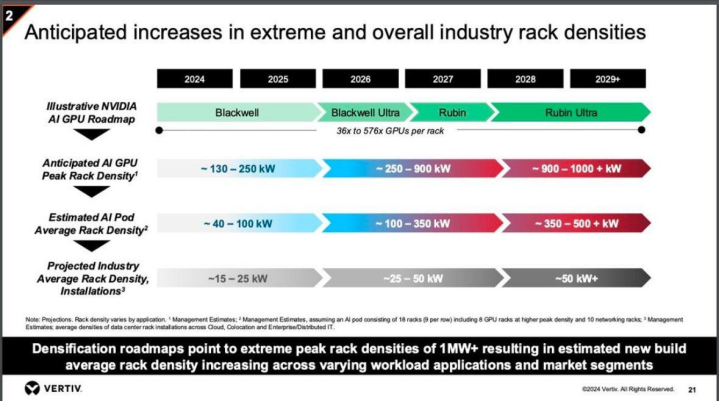
(Figure 1. AI Cluster Rack Power Density Scaling Trend)
1.1 Copper and mechanical constraints
A 1 MW, 54 V system requires ~200 kg of copper busbar infrastructure.
This level of conductor mass introduces mechanical constraints and directly reduces usable rack volume for compute, interconnect, and liquid cooling systems.
1.2 Resistive loss scaling
Power loss follows I²R scaling.
At high current levels, distribution losses become a primary thermal load and must be continuously removed at rack scale.
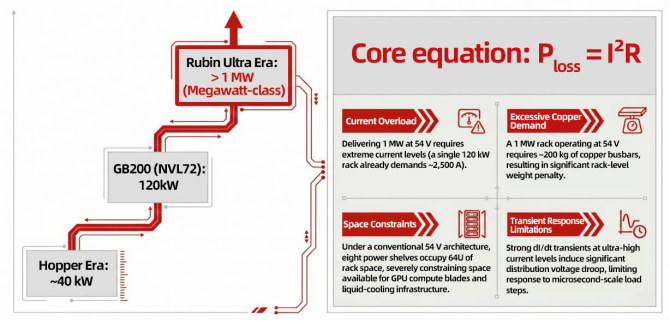
(Figure 2. Physical Constraints Driving the Transition to 800 V HVDC)
1.3 Transient response limitation
AI training workloads introduce microsecond-scale load transients.
At high current and low voltage, systems exhibit voltage droop and inductive effects under high dI/dt conditions.
Transient stability becomes a system-level constraint.
2. Transition to 800 V HVDC Architecture
Increasing distribution voltage to 800 V HVDC reduces current proportionally for equivalent power delivery.
This change alters system-level power distribution behavior.
2.1 Conductor reduction
800 V HVDC enables ~45% reduction in copper usage compared to 54 V architectures.
This improves rack-level mechanical integration and increases usable volume for compute subsystems.
2.2 System efficiency improvement
Reduction of multi-stage AC/DC conversion paths enables up to ~5% improvement in end-to-end power efficiency.
2.3 Cooling and subsystem simplification
Lower current reduces PSU count and associated thermal overhead.
Cooling demand can be reduced by up to ~30% depending on system configuration.
2.4 DC-bus energy buffering
800 V HVDC enables direct integration of battery backup units (BBU) and energy storage systems on the DC bus.
This enables local peak shaving during GPU load transients and reduces stress on upstream power infrastructure.
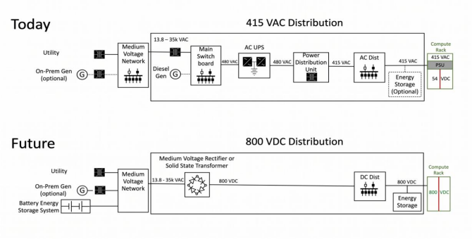
(Figure 3. Evolution of AI Data Center Power Distribution Architecture)
3. Power conversion hierarchy
AI accelerators require sub-1 V core supply voltage, requiring a multi-stage conversion chain.
3.1 10 kV AC → 800 V DC (facility level)
Solid-state transformers (SST) or medium-voltage rectification systems replace traditional transformer-based architectures.
Silicon carbide (SiC) devices enable direct conversion from medium-voltage AC to 800 V DC with efficiency above 98%.
3.2 800 V DC → 48 V / 54 V DC (rack level)
Rack-level power is implemented through sidecar architectures, separating power conversion from compute infrastructure.
High-ratio LLC resonant converters operate under ZVS/ZCS conditions to reduce switching losses.
3.3 48 V DC → 12 V DC (board level)
Gallium nitride (GaN) devices operating in the MHz switching range enable high-density conversion.
Higher switching frequency reduces passive component size and increases power density.
3.4 12 V DC → sub-1 V GPU rail (point-of-load)
GPU power delivery requirements reach multi-kiloampere current levels at sub-1 V voltage.
Lateral power delivery (LPD) is replaced by vertical power delivery (VPD).
VRM modules are placed directly beneath the GPU package.
Electrical path length is reduced to millimeter scale.
Power delivery efficiency improves by ~5%.
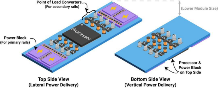
(Figure 4. Comparison of Lateral and Vertical Power Delivery Architectures)
4. Reliability constraints in 800 V systems
800 V HVDC introduces new failure modes across the power delivery chain.
4.1 DC arc risk
At 800 V DC, the absence of zero-crossing increases arc persistence under fault conditions.
4.2 High dV/dt isolation stress
SiC and GaN switching devices generate high dV/dt transitions.
4.3 Thermal co-location in VPD architectures
Power stages are placed within millimeters of high-power GPUs.
Thermal density becomes concentrated in sub-2 mm vertical stack regions.
5. Semiconductor reliability as a system dependency
Acroview Technology’s V9000 automated ABI burn-in platform is designed for high-volume stress validation of power devices used in AI infrastructure.

Key capabilities include:
- Parallel burn-in testing of 512+ devices under test (DUTs)
- Independent closed-loop thermal control per DUT
- Up to 1200 A steady-state load simulation
- Controlled high-stress electrical and thermal aging conditions
The system enables detection of early-life failures prior to package- and board-level integration.
Conclusion
800 V HVDC represents a structural transition in AI infrastructure power architecture.
As system power scales toward megawatt-class racks, power delivery becomes a primary architectural constraint.
System scalability is determined by the integrity of the full power chain, from semiconductor-level validation to rack-scale distribution.
Reliability across this chain is a prerequisite for continued scaling of AI compute infrastructure.
- Previous: "AI Dreams, A 'Core' Future" – The 2025 ACROVIEW Annual Gala Concludes Successfully
- Next: No More!
- 7F, Hanking Center (SOMA) 9968 Shennan Avenue, Nanshan Dist, Shenzhen, 518052, P.R.C
- sales@acroview.com