
Acroview technology
Vertical Power Delivery (VPD) in AI Systems
1. Introduction
In advanced AI compute systems, power delivery is increasingly a primary design constraint alongside compute density and memory bandwidth. As GPU architectures scale toward higher parallelism and increased workload intensity, device-level current demand is reaching kiloampere-class operating regimes.
At these operating points, conventional planar power delivery networks (PDNs) exhibit increasing limitations related to resistive loss, loop inductance, and spatial routing constraints within the printed circuit board (PCB) stack-up.
Vertical Power Delivery (VPD) is an architectural approach that modifies the spatial organization of the PDN by relocating power conversion stages to the backside of the PCB and implementing vertical current transfer paths through the board stack-up.
2. Limitations of Lateral Power Delivery (LPD) Architectures
In conventional GPU and accelerator platforms, power delivery is typically implemented using a lateral distribution topology. Voltage regulator modules (VRMs) or point-of-load (POL) converters are placed around the periphery of the GPU package, with power routed through lateral copper planes and redistribution layers.
As current levels increase, several physical constraints become more pronounced:
2.1 Conduction loss and thermal density
At high current magnitudes (kiloampere-scale), even short lateral routing paths introduce measurable I²R losses. This results in localized thermal density increase within the PCB stack-up and associated thermal management complexity.
2.2 Transient response limitations
AI training and inference workloads exhibit high di/dt characteristics. Lateral PDN topologies introduce additional parasitic inductance and resistance, which increase voltage droop and extend settling time under fast load transients.
2.3 Routing and placement constraints
Modern GPU packages are co-designed with high-bandwidth memory (HBM) stacks and high-speed I/O interfaces. This significantly reduces available perimeter routing area for power conversion components, limiting scalability of peripheral VRM placement.
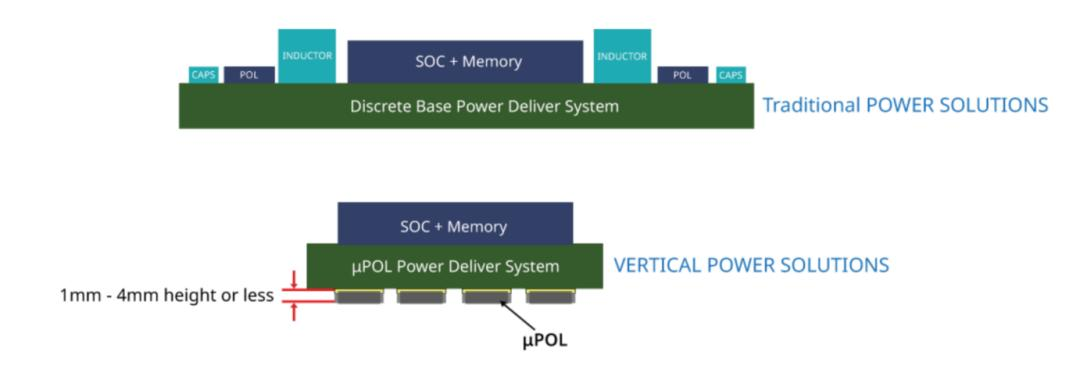
(Figure 1. Conventional Power Delivery vs. Vertical Power Delivery (VPD))
3. Vertical Power Delivery (VPD) Architecture
Vertical Power Delivery modifies the PDN topology by relocating power conversion stages (VRM / POL) to the backside of the PCB, aligned with the processor package footprint. Electrical energy is delivered through vertical interconnect structures within the PCB stack-up rather than through extended lateral routing.
3.1 Electrical path characteristics
The effective current path length is reduced from lateral centimeter-scale routing to millimeter-scale vertical conduction through the board stack-up, reducing conduction resistance and associated I²R losses.
3.2 Loop inductance reduction
The vertical current path reduces power loop inductance, which improves transient response under high di/dt load conditions commonly observed in large-scale AI workloads.
3.3 Front-side layout decoupling
Relocation of power stages to the backside of the PCB reduces component density around the GPU package on the primary side, increasing available routing area for HBM interfaces and high-speed signal integrity (SI) channels.
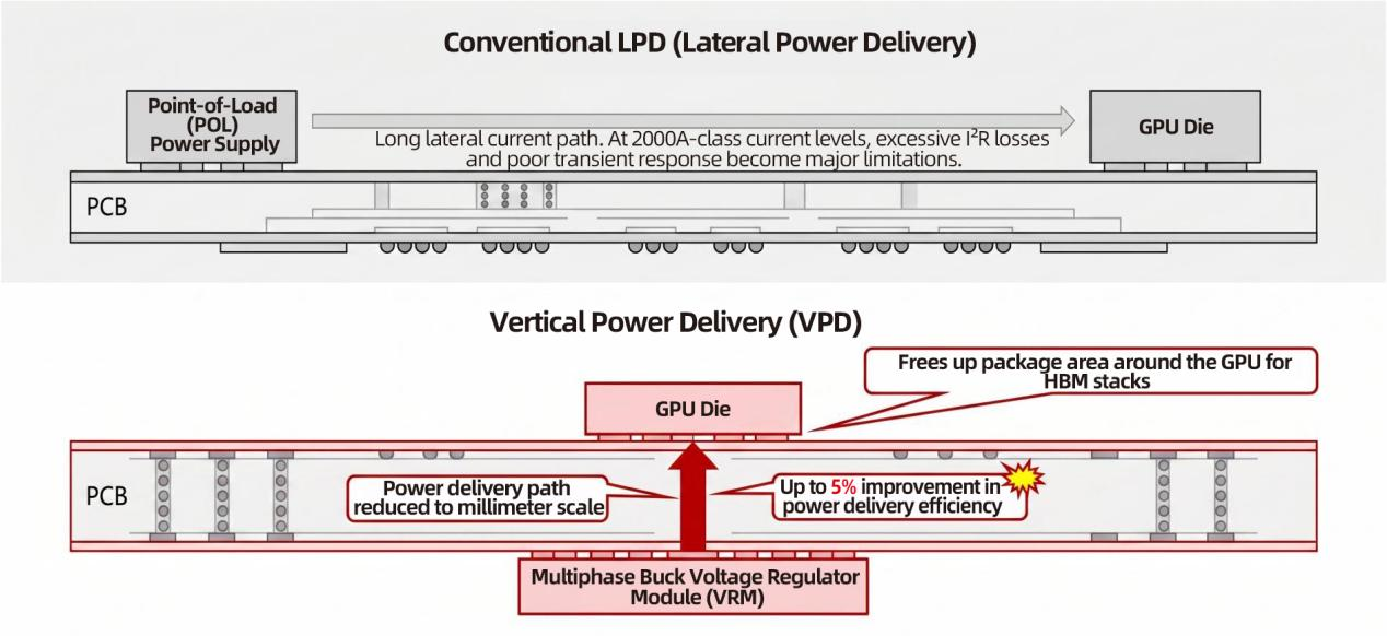
(Figure 2. 3D Comparison of Lateral Power Delivery (LPD) and Vertical Power Delivery (VPD))
4. Industry Architecture Direction (Publicly Discussed Design Trends)
Vertical power delivery concepts are increasingly referenced in next-generation high-performance computing (HPC) and AI accelerator platform discussions.
In publicly available architectural discussions of future GPU platforms (including NVIDIA Rubin-class system designs), vertically integrated power delivery is being evaluated as a potential approach to address scaling constraints in power density and package integration.
Across the semiconductor ecosystem, system designers, hyperscale data center operators, and device vendors are evaluating variations of vertical PDN architectures as power density continues to increase.
On the power conversion side, vendors such as Monolithic Power Systems (MPS) and Vicor Corporation are developing high-density, low-footprint power modules optimized for reduced parasitic impedance and improved placement flexibility within constrained board environments.
5. System-Level Thermal Coupling Considerations
While VPD improves electrical path efficiency and spatial utilization, it introduces increased vertical thermal coupling within the system stack-up.
By relocating power conversion stages to the backside of the PCB, directly opposite the GPU thermal zone, thermal domains between compute and power stages become more closely coupled.
This configuration increases local heat flux density and reduces thermal isolation within the stack-up, requiring system-level co-design of mechanical structure, cooling solution, and power stage thermal dissipation.
6. Reliability Validation in High Current-Density Power Systems
In VPD-based architectures, power delivery subsystems become tightly coupled to system-level reliability requirements.
Acroview develops automated burn-in and reliability stress platforms for high-power semiconductor devices used in advanced AI power delivery systems.
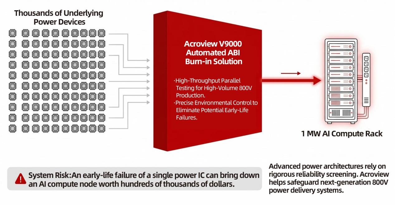
(Figure 3. Acroview V9000 Automated ABI Burn-in Solution)
These platforms are designed to support:
· High-parallel device stress execution for production-scale validation
· Controlled high-current electrical loading conditions representative of AI PDN operating regimes
· Combined thermal and electrical stress profiles to evaluate early-life failure mechanisms under accelerated conditions
The objective of such systems is to provide characterization and screening capability for power devices prior to integration into high-density compute power delivery networks.
7. Conclusion
At high current-density regimes, power delivery architecture becomes a primary constraint in system-level design of AI computing platforms. Vertical Power Delivery represents one class of architectural approach that addresses limitations in lateral routing-based PDNs by introducing vertical current transfer paths and backside power integration.
As system integration density increases, power delivery design, thermal coupling, and signal integrity considerations must be treated as co-optimized parameters within the overall platform architecture.
Reliability validation of high-current power components remains a critical requirement in supporting stable operation of large-scale AI compute infrastructure.

- 7F, Hanking Center (SOMA) 9968 Shennan Avenue, Nanshan Dist, Shenzhen, 518052, P.R.C
- sales@acroview.com