
Acroview technology
HBM Reliability at Scale: Addressing Advanced Memory Testing Challenges
High-bandwidth memory (HBM) has become a critical memory technology for the next generation of artificial intelligence (AI) computing and high-performance computing (HPC) systems. As AI workloads continue to expand, the demand for higher memory bandwidth, improved power efficiency, and long-term system reliability is accelerating the evolution of advanced memory architectures.

However, moving HBM from engineering validation into high-volume manufacturing requires more than advances in memory design and packaging technologies. A scalable HBM ecosystem also depends on reliable production processes and advanced validation capabilities that can identify latent defects before devices are deployed in demanding computing environments.
The transition from initial technology development to large-scale commercial deployment depends on one often underestimated factor: manufacturing reliability validation.
For HBM, achieving high performance is only the beginning. Ensuring long-term reliability under intensive thermal, electrical, and mechanical stress conditions is essential for successful adoption in AI infrastructure.
HBM: A Critical Memory Architecture for AI Computing
If GPUs serve as the computing engines of AI systems, HBM functions as the high-speed memory architecture that enables these processors to fully utilize their computational capabilities.
Unlike conventional DRAM architectures, where memory dies are placed side-by-side on a PCB, HBM vertically stacks multiple DRAM layers and connects them through through-silicon vias (TSVs) and micro-bumps. These stacked memory devices are then integrated with GPUs or CPUs through advanced 2.5D packaging technologies using silicon interposers.
This architecture enables significantly higher memory bandwidth while reducing physical footprint and improving power efficiency compared with traditional memory solutions.
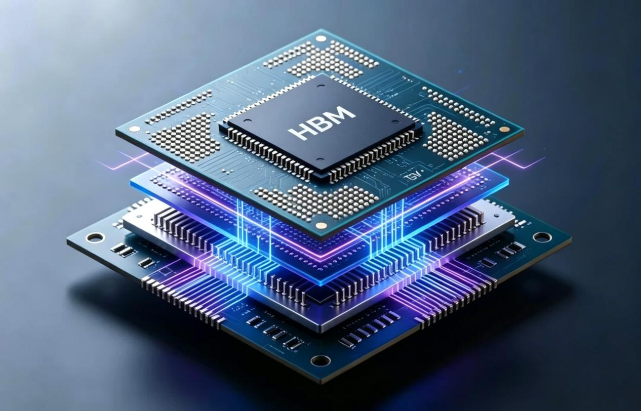
Since the introduction of the first-generation HBM with AMD Radeon R9 Fury products in 2015, HBM has evolved rapidly. Originally introduced as an advanced feature for high-end graphics applications, HBM has evolved into a fundamental component of AI accelerators and high-performance computing platforms.
With the development of the HBM4 standard, featuring a 2048-bit interface, up to 16-layer stacking, and bandwidth exceeding 2 TB/s per stack, HBM continues to push the limits of memory performance.
However, every increase in architectural complexity introduces new manufacturing and reliability challenges.
The Reliability Challenges Behind HBM Scaling
The stacked structure that enables HBM’s exceptional bandwidth also creates additional reliability risks.
Unlike traditional memory packages, where individual components can be independently tested, HBM integrates multiple memory dies into a single high-value package. A defect in a single layer or interconnect can potentially affect the reliability of the entire stack.
Several failure mechanisms become increasingly critical as HBM technology advances:
· TSV interconnect failures, including open and short defects caused by manufacturing variation or long-term stress;
· Micro-bump degradation, where repeated thermal cycling and mechanical stress may affect contact reliability;
· Thermal-induced stress, caused by differences in material expansion within complex stacked structures;
· Long-term electrical degradation, resulting from continuous high-performance operation.
Many of these defects are difficult to identify during conventional component-level testing. However, under extended operation in AI servers and data center environments, these latent failures may eventually impact system availability and reliability.
As a result, HBM reliability testing can no longer be treated as a final inspection step after manufacturing. Instead, reliability validation must become an integrated process across the entire production lifecycle, including wafer-level testing, known good die (KGD) screening, stacking, packaging, and final qualification.
The timing of defect detection also has a direct impact on manufacturing cost.
If a failure is discovered after stacking and packaging, the entire HBM assembly may need to be discarded, resulting in significant material and production losses. By identifying potential failures earlier during the KGD stage, manufacturers can improve yield management and reduce unnecessary downstream costs.
This makes advanced burn-in testing an essential part of HBM production.
Advanced Burn-In Testing: A Foundation for HBM Production Reliability
Burn-in testing accelerates the detection of latent defects by applying controlled electrical and thermal stress conditions that exceed normal operating environments.
For HBM devices, this process is particularly important because many reliability issues are associated with long-term exposure to temperature variation, electrical loading, and mechanical stress.
By applying accelerated stress conditions before shipment, manufacturers can identify early-life failures and improve confidence in long-term device reliability.
As HBM generations continue to evolve toward higher stack densities, greater bandwidth, and increased power consumption, conventional testing approaches face limitations in:
· parallel testing efficiency;
· thermal environment control;
· mechanical contact stability;
· automation capability;
· test flexibility for different device generations.
To support next-generation HBM manufacturing, reliability validation platforms must provide both high test coverage and production scalability.
Acroview V9000-HBM-T: A Production-Oriented Reliability Validation Platform
The Acroview V9000-HBM-T automatic three-temperature burn-in test system is designed to address the reliability validation requirements of advanced HBM production.
Rather than functioning as a standalone inspection tool, the platform is developed around a production-oriented approach that integrates high-throughput testing, automated operation, precision environmental control, and flexible test capability.
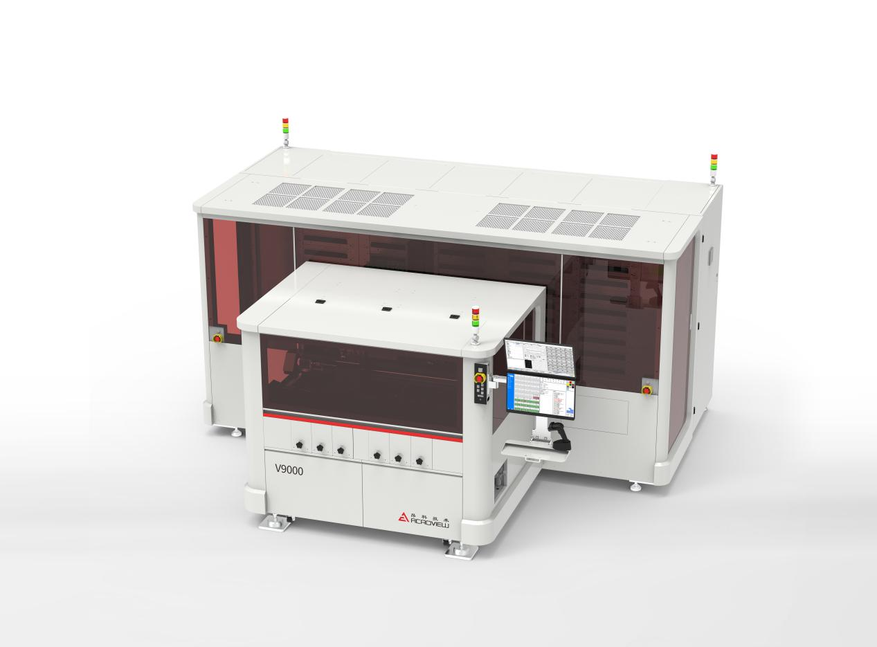
Its architecture is designed to support both engineering validation and high-volume manufacturing environments, helping manufacturers improve testing efficiency while maintaining reliability coverage.
Engineering Capabilities for High-Volume HBM Testing
High-Parallel Test Architecture for Production Efficiency
One of the key challenges in HBM manufacturing is balancing comprehensive reliability validation with production throughput.
The V9000-HBM-T supports simultaneous testing of up to 1,920 devices, enabling high-parallel testing capability for long-duration burn-in processes.
By increasing the number of devices tested within each cycle, the system helps reduce average test time per device and improve overall production efficiency, particularly for HBM applications requiring extended reliability stress testing.
The same hardware platform can support both engineering development and production deployment, reducing the need for major equipment changes during product transition.
Fully Automated Workflow for Consistent and Traceable Testing
Manual handling processes can introduce variations in device contact conditions, transportation procedures, and operational consistency.
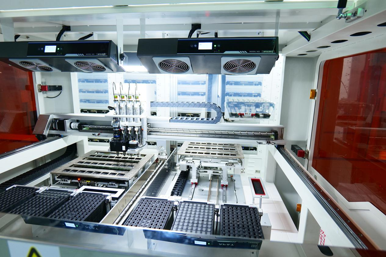
The V9000-HBM-T integrates automated loading and unloading, BIB (burn-in board) transfer management, and automated sorting capability to create a fully automated testing workflow.
The system supports multiple reliability test processes, including:
· High Temperature Operating Life (HTOL);
· Low Temperature Operating Life (LTOL);
· Burn-In (BI) testing.
By minimizing manual intervention, the platform helps reduce operational variability and maintain consistent test conditions.
In addition, testing data is continuously collected and associated with device and batch information, enabling full traceability throughout the validation process. This allows manufacturers to analyze failure conditions and improve production processes through data-driven optimization.
Precision Thermal and Mechanical Control for Accelerated Stress Testing
HBM reliability failures are often associated with thermal expansion, mechanical stress, and interconnect degradation.
To effectively identify these potential issues, burn-in systems must provide accurate and stable stress environments.
The V9000-HBM-T features independent closed-loop control systems for temperature and mechanical pressure management:
· The thermal control system supports a temperature range from -40°C to 150°C, with temperature accuracy within ±3°C, enabling controlled simulation of different operating environments.
· The independent pressure servo system maintains device-to-test-board contact pressure accuracy within 5%, improving contact stability and reducing false failures caused by unstable electrical connections.
The system also monitors multiple environmental parameters, including device operating conditions, chamber condensation status, and temperature/pressure variations, allowing dynamic adjustment of testing conditions and improving measurement consistency.
Flexible Test Architecture for Multiple HBM Generations
HBM technology continues to evolve rapidly, with increasing stack heights, higher signal speeds, and more demanding reliability requirements.
A fixed testing architecture may not be sufficient to support future device generations.
The V9000-HBM-T integrates Acroview’s proprietary test system architecture, featuring configurable test modules and programmable power measurement units (PPMU) to support different HBM specifications and validation requirements.
The system incorporates an Algorithmic Pattern Generator (ALPG) module with logic test vector depth of up to 128M, enabling comprehensive validation of:
· high-speed signal transmission;
· long-term voltage and current stress;
· read/write endurance performance.
Its flexible hardware and software architecture allows manufacturers to adapt testing configurations as HBM technologies continue to advance.
Preparing for Future HBM Validation Requirements
As the semiconductor industry moves from HBM2e toward HBM3E and future HBM4 architectures, reliability testing requirements will continue to increase.
Higher stacking density, greater power consumption, and more complex packaging structures require advanced validation solutions capable of supporting both current production needs and future technology transitions.
The V9000-HBM-T platform is designed to support continued development in areas including:
· dynamic burn-in testing;
· digital traceability across manufacturing processes;
· higher-power parallel testing;
· scalable automation expansion.
Through continuous improvement in test efficiency, defect detection capability, and production adaptability, advanced reliability validation can help manufacturers accelerate the transition from technology development to stable production.
Conclusion
The commercialization of HBM requires more than advances in memory architecture and packaging technology. It also depends on the ability to consistently validate device reliability under demanding operating conditions.
From wafer-level screening to final reliability testing, every stage of the manufacturing process contributes to the success of high-performance memory products.
The Acroview V9000-HBM-T three-temperature burn-in test system provides a production-focused approach to HBM reliability validation, combining high parallel testing capability, automation, precision environmental control, and flexible test architecture.
As AI computing and HPC systems continue to drive demand for higher memory performance, reliable manufacturing validation will remain an essential element in enabling the next generation of high-bandwidth memory technologies.

- 7F, Hanking Center (SOMA) 9968 Shennan Avenue, Nanshan Dist, Shenzhen, 518052, P.R.C
- sales@acroview.com